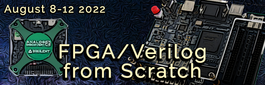
|
Each day is composed of theoretical lectures (CX.X) and the experimental application of what has been learned
(LX.X).
Day 1: Digital
Design Primer
- C1.1:
Logic gates, truth table
- C1.2:
Writing boolean equation, k-map and solving an example
- C1.3:
FPGA definition, usage areas and importance
- C1.4:
Schematic and RTL simulation, running on FPGA
- L1.1:
Intel Quartus tutorial: design schematic, run on RTL & FPGA, FPGA I/O
Day 2: Verilog for
Hardware Design
- C2.1:
HDL Intro, Verilog - structural
- C2.2:
Verilog- dataflow
- C2.3:
Verilog design example
- C2.4:
Writing a testbench for Modelsim
- L2.1:
Design with Verilog, Write Testbench, Simulate and Test on FPGA
Day 3: FSM
Primer
- C3.1:
FSM introduction
- C3.2:
FSM examples
- C3.3:
FSM Design: State Diagram, Truth Table, Boolean Expressions
- C3.4:
FSM Design using structural and dataflow Verilog
- L3.1:
Intel Quartus Application of FSM Design
Day 4: Advanced
FSM
- C4.1:
Behavioral Verilog
- C4.2:
FSM design using behavioral Verilog
- C4.3:
Advanced Testbench Writing and I/O
- L4.1:
Design and simulate FSM using behavioral Verilog and Modelsim
- L4.2:
FPGA Upload, USB Oscilloscope Testing
Day 5: Case
Study: From C to FPGA
- C5.1:
From C to Algorithmic State Machine (ASM)
- C5.2:
ASM Optimization and Datapath Construction
- C5.3:
ASM Implementation with Behavioral Verilog
- C5.4:
Simulate and Upload to FPGA
- L5.1:
A C function fully implemented with Verilog
- L5.2:
Simulated with Modelsim
- L5.3:
Uploaded to FPGA, tested with Oscilloscope
|